Description
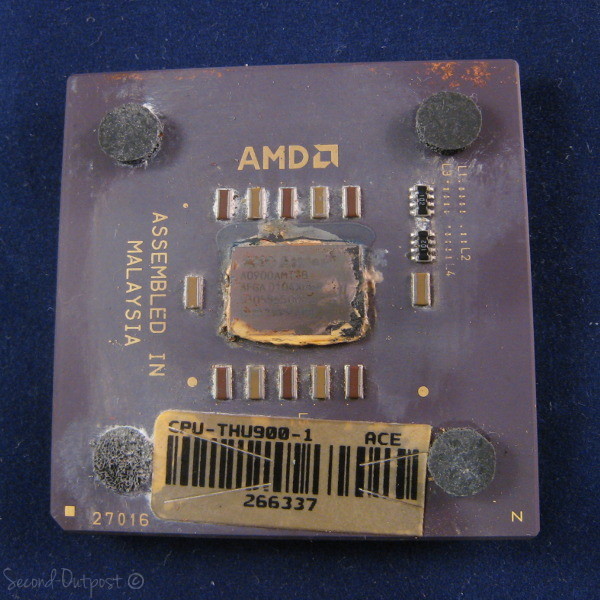
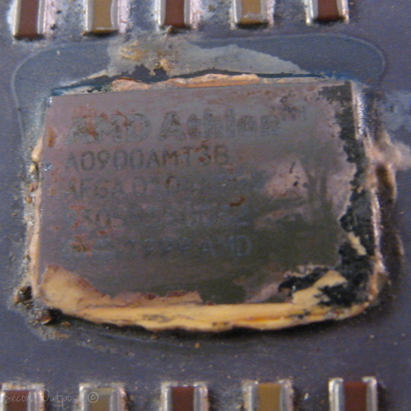
This is a used AMD Athlon CPU A0900AMT3B in good working condition.
General information – A0900AMT3B |
|
| Type | CPU / Microprocessor |
| Market segment | Desktop |
| Family | AMD Athlon |
| CPU part number |
|
| Stepping codes | ADFA AFFA AGGA AQFA |
| Frequency | 900 MHz |
| Bus speed | 200 MHz |
| Clock multiplier | 8 |
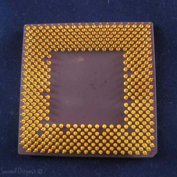
| Package | 453-pin staggered ceramic PGA 1.95″ x 1.95″ (4.95 cm x 4.95 cm) |
| AMD Package number | 26822 |
| Socket | Socket A (Socket 462) |
Architecture / Microarchitecture |
|
| Microarchitecture | K7 |
| Processor core | Thunderbird (Model 4) |
| Manufacturing process | 0.18 micron 37 million transistors |
| Die size | 120mm2 |
| Data width | 32 bit |
| The number of CPU cores | 1 |
| The number of threads | 1 |
| Floating Point Unit | Integrated |
| Level 1 cache size | 64 KB 2-way set associative code cache 64 KB 2-way set associative data cache |
| Level 2 cache size | Full-speed on-die 256 KB |
| Multiprocessing | Uniprocessor |
| Features |
|
| Low power features |
|
| Integrated peripherals / components | |
| Integrated graphics | None |
| Electrical / Thermal parameters | |
| V core | 1.75V |
| Minimum/Maximum operating temperature | 0°C – 90°C |
Notes on AMD A0900AMT3B Athlon 900 MHz |
|
|
|
The Athlon Archetechure:
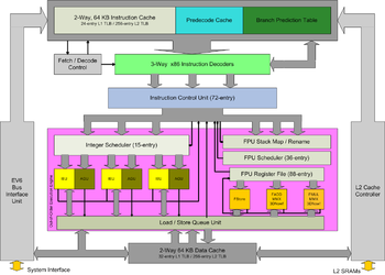
Internally, the Athlon is a fully seventh generation x86 processor, the first of its kind. Like the AMD K5 and K6, the Athlon dynamically buffers internal micro-instructions at runtime resulting from parallel x86 instruction decoding. The CPU is an out-of-order design, again like previous post-5×86 AMD CPUs. The Athlon utilizes the Alpha 21264’s EV6 bus architecture with double data rate (DDR) technology. This means that at 100 MHz, the Athlon front side bus actually transfers at a rate similar to a 200 MHz single data rate bus (referred to as 200 MT/s), which was superior to the method used on Intel’s Pentium III (with SDR bus speeds of 100 MHz and 133 MHz).
For the A0900AMT3B, AMD designed the CPU with more robust x86 instruction decoding capabilities than that of K6, to enhance its ability to keep more data in-flight at once. The Athlon’s three decoders could potentially decode three x86 instructions to six microinstructions per clock, although this was somewhat unlikely in real-world use. The critical branch predictor unit, essential to keeping the pipeline busy, was enhanced compared to what was on board the K6. Deeper pipelining with more stages allowed higher clock speeds to be attained. Whereas the AMD K6-III+ topped out at 570 MHz due to its short pipeline, even when built on the 180 nm process, the Athlon was capable of clocking much higher.
New Floating-Point Unit
AMD ended its long-time handicap with floating point x87 performance by designing a super-pipelined, out-of-order, triple-issue floating point unit. Each of its three units was tailored to be able to calculate an optimal type of instructions with some redundancy. By having separate units, it was possible to operate on more than one floating point instruction at once. This FPU was a huge step forward for AMD. While the K6 FPU had looked anemic compared to the Intel P6 FPU, with Athlon this was no longer the case.
The 3DNow! floating point SIMD technology, again present, received some revisions and a name change to “Enhanced 3DNow!”. Additions included DSP instructions and an implementation of the extended MMX subset of Intel SSE.
The Athlon’s CPU cache consisted of the typical two levels. Athlon was the first x86 processor with a 128 kB split level 1 cache; a 2-way associative cache separated into 2×64 kB for data and instructions (a concept from Harvard architecture). This cache was double the size of K6’s already large 2×32 kB cache, and quadruple the size of Pentium II and III’s 2×16 kB L1 cache. The initial Athlon (Slot A, later called Athlon Classic) used 512 kB of level 2 cache separate from the CPU, on the processor cartridge board, running at 50% to 33% of core speed. This was done because the 250 nm manufacturing process was too large to allow for on-die cache while maintaining cost-effective die size. Later Athlon CPUs, afforded greater transistor budgets by smaller 180 nm and 130 nm process nodes, moved to on-die L2 cache at full CPU clock speed.

